
Solution Overview
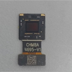
Chip offset and tilt are key control points in semiconductor packaging. Deviation will cause bonding failure and lower yield. Manual inspection cannot meet high-precision mass production requirements.
This solution adopts COBEKK AG Series Semiconductor Packaging 3D Measuring Machine, paired with self-developed AG-ISOBIT measurement software:
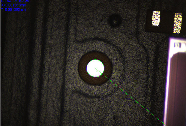
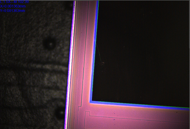
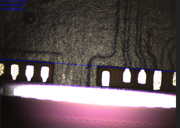
·DA & LHA-IR dual imaging modes, adaptable to different chip surfaces and substrates
·Synchronously capture X/Y offset, rotation angle and corner height
·Auto OK/NG judgment and statistical report export
1.Dual imaging modes: DA and LHA-IR optional for diverse packaging materials
2.Multi-parameter synchronous measurement: offset, angle and inclination in one capture
3.Automatic OK/NG judgment to avoid human misjudgment
4.Export statistical reports for quality traceability
5.Self-developed AG-ISOBIT software, easy programming for batch testing
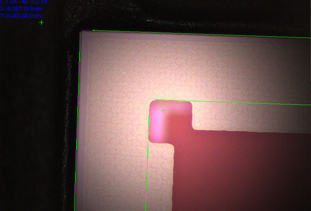
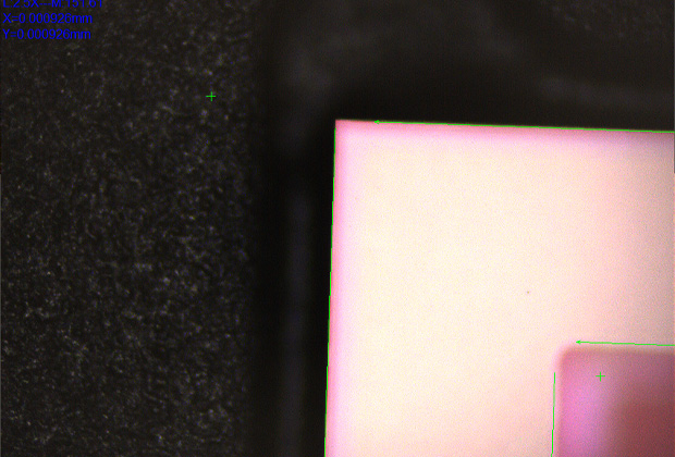
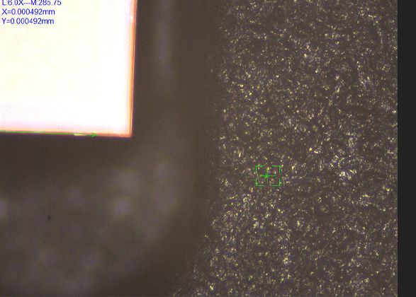
Tests were carried out under DA and LHA-IR modes with the same tolerance.
DA mode: Samples within tolerance, marked OK.
LHA-IR mode: Partial samples out of tolerance, marked NG.
The comparison helps select the best imaging scheme for stable mass inspection.
DA test results
| Masurium | Angle | X biased | Y biased | Hht1 | Hht2 | Hht3 | Hht4 | Incline |
| Feature name | Angle | X distance | Y distance | Altitude | Altitude | Altitude | Altitude | Result1 |
| Standard value | 0 | 457.3 | 36.1 | 190 | 190 | 190 | 190 | 0 |
| Upper tolerance | 0.05 | 20 | 20 | 50 | 50 | 50 | 50 | 30 |
| Lower tolerance | -0.05 | -50 | -20 | -50 | -50 | -50 | -50 | -30 |
| Specification upper limit | 0.05 | 477.3 | 56.1 | 240 | 240 | 240 | 240 | 30 |
| Specification lower limit | -0.05 | 407.3 | 16.1 | 140 | 140 | 140 | 140 | -30 |
| Maximum value | 0.0418 | 475.1676 | 30.2889 | 222.9996 | 209.4955 | 215.4999 | 223.5031 | 24.5056 |
| Minimum value | 0.0234 | 468.9463 | 18.1535 | 195.5032 | 199.4934 | 198.9975 | 196.4951 | 14.4959 |
| Average value | 0.030066667 | 471.458 | 24.43916 | 207.0007333 | 203.3309667 | 209.1649333 | 209.1649333 | 18.8319 |
| Range | 0.0184 | 6.2213 | 12.1354 | 27.4964 | 10.0021 | 16.5024 | 27.008 | 10.0097 |
| OK | 0.025 | 468.9463 | 30.2889 | 202.4994 | 201.004 | 215.4999 | 207.4966 | 14.4959 |
| OK | 0.0234 | 470.2601 | 18.1535 | 195.5032 | 209.4955 | 212.9974 | 196.4951 | 17.4942 |
| OK | 0.0418 | 475.1676 | 24.8751 | 222.9996 | 199.4934 | 198.9975 | 223.5031 | 24.5056 |
| Masurium | Angle | X biased | Y biased | Hht1 | Hht2 | Hht3 | Hht4 | Incline |
| Feature name | Angle | X distance | Y distance | Altitude | Altitude | Altitude | Altitude | Result1 |
| Standard value | 0 | 457.3 | 36.1 | 190 | 190 | 190 | 190 | 0 |
| Upper tolerance | 0.05 | 20 | 20 | 50 | 50 | 50 | 50 | 30 |
| Lower tolerance | -0.05 | -50 | -20 | -50 | -50 | -50 | -50 | -30 |
| Specification upper limit | 0.05 | 477.3 | 56.1 | 240 | 240 | 240 | 240 | 30 |
| Specification lower limit | -0.05 | 407.3 | 16.1 | 140 | 140 | 140 | 140 | -30 |
| Maximum value | 0.0418 | 475.1676 | 30.2889 | 222.9996 | 209.4955 | 215.4999 | 223.5031 | 24.5056 |
| Minimum value | 0.0234 | 468.9463 | 18.1535 | 195.5032 | 199.4934 | 198.9975 | 196.4951 | 14.4959 |
| Average value | 0.030066667 | 471.458 | 24.43916 | 207.0007333 | 203.3309667 | 209.1649333 | 209.1649333 | 18.8319 |
| Range | 0.0184 | 6.2213 | 12.1354 | 27.4964 | 10.0021 | 16.5024 | 27.008 | 10.0097 |
| NG | 0.025 | 468.9463 | 30.2889 | 202.4994 | 201.004 | 215.4999 | 207.4966 | 14.4959 |
| NG | 0.0234 | 470.2601 | 18.1535 | 195.5032 | 209.4955 | 212.9974 | 196.4951 | 17.4942 |
| NG | 0.0418 | 475.1676 | 24.8751 | 222.9996 | 199.4934 | 198.9975 | 223.5031 | 24.5056 |
The AG Series Semiconductor Packaging 3D Measuring Machine is suitable for chip offset and inclination inspection in semiconductor packaging. Dual-mode design adapts complex surface conditions, replaces manual inspection and satisfies mass quality control.
Semiconductor packaging, IC assembly, chip bonding inspection, microelectronics manufacturing
